Using PLL for a faster clock
The counter works but 12MHz is quite slow for a lot of operations, including generating video signals.
FPGAs come with specialized logic blocks I can instantiate in my design and use them as any other verilog module. They have parameters, inputs and outputs and they offer various functions like SPI, I2C, RAM, SERDES or PLL. They are called primitives.
Tipically these PLL blocks have an voltage-controlled oscillator (VCO) with a very high frequency, in case of ICE40 it has to run between 533MHz and 1066MHz. After VCO settles to a specific frequency in this range, a divider can generate smaller frequencies which can be sustained by all the other elements of the design together. The range for the actual output clock frequency for this PLL are 16MHz to 275MHz.
Even though PLL can generate such high frequencies it doesn’t mean my FPGA will be able to function at 275MHz. The datasheet mentions for example that a global buffer clock network has a maximum frequency of 185MHz. YMMV but in general the design and hardware limitations will dictate the max speed.
For now I will try to focus on how to instantiate a PLL primitive in my code.
Instantiate the PLL
Lattice offers a datasheet for ICE40 UltraPlus and also a PDF file named “Technology Library”. In this later file all the available specialized logic blocks are described along with their parameters and I/Os.
All the files can be found by accessing this url: http://www.latticesemi.com/en/Products/FPGAandCPLD/iCE40UltraPlus
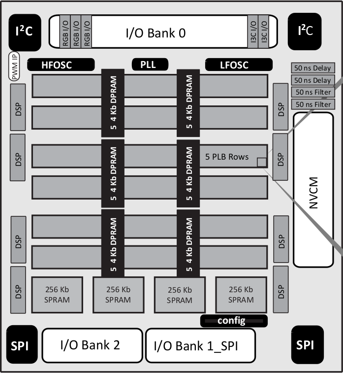
ICE40 UltraPlus has three sysIO banks, one on top and two at the bottom. Bank 1 cannot be used for clock input.
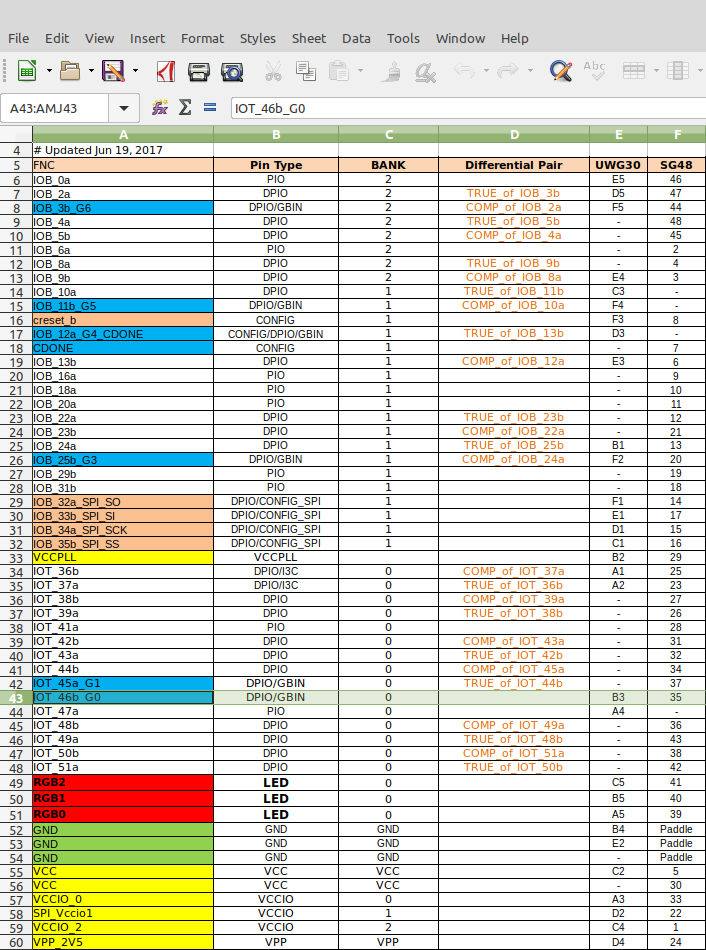
Since the 12MHz external clock going in the chip on the icebreaker board is connected to pin 35, according to the datasheet it means it’s connected to IOT_46b_G0
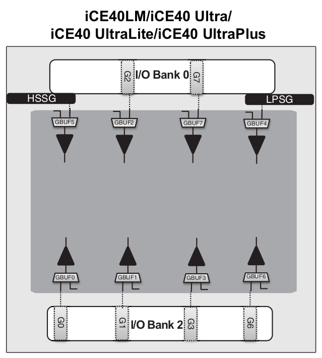
G0 is connected to I/O bank 2 according to the following diagram:
Now, in to the technology library datasheet I can see all the PLL primitives I have available:
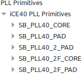
SB_PLL40_CORE should be used when the clock source of the PLL is driven by an input pad that is in the upper I/O bank.
SB_PLL40_PAD should be used if the clock source of the PLL is driven by an input that is in the upper or lower I/O banks (0 or 2). In this case it is in the lower bank so I need to use this primitive. Here is its building block according to the technology library:
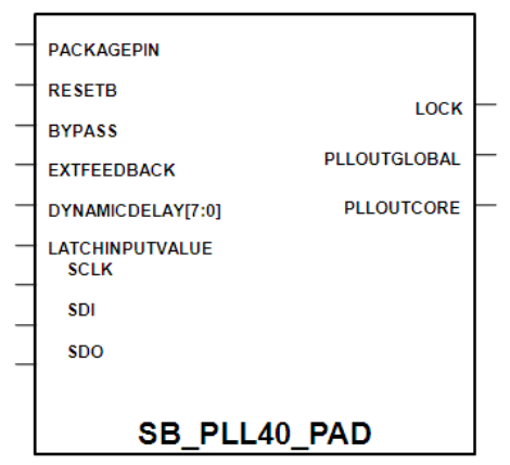
Best explanation of these parameters is given in the Lattice PDF, I will talk about the most important signals only
Inputs
- PACKAGEPIN is the source clock serving as input to this primitive
Outputs
- LOCK is indicating when the signal on the out pin is locked to the PLL source of the reference clock
- PLLOUTGLOBAL is the output clock generated by the PLL and it drives a global clock network on the FPGA
- PLLOUTCORE is the output clock generated by the PLL but drives regular FPGA routing.
Depending on the needs a design would use either PLLOUTCORE or PLLOUTGLOBAL.
Primitive parameters
Best way to understand what all these mean is to read Lattice’s technology library PDF. I will talk about the one which matters in this simple example.
- FEEDBACK_PATH: set to SIMPLE (fb is internally connected to VCO)
The following 4 parameters are the most important ones and decide what the output frequency will be. They can be calculated using icepll tool which takes an input frequency and an output frequency and calculates the values
To get the values for 100MHz output from the 12MHz input clock I issue the following command:
icepll -i 12 -o 100
Calculated parameters are:
F_PLLIN:    12.000 MHz (given)
F_PLLOUT:  100.000 MHz (requested)
F_PLLOUT:  100.500 MHz (achieved)

FEEDBACK: SIMPLE
F_PFD:   12.000 MHz
F_VCO:  804.000 MHz

DIVR:  0 (4'b0000)
DIVF: 66 (7'b1000010)
DIVQ:  3 (3'b011)

FILTER_RANGE: 1 (3'b001)
It can get very close to 100 (in this case 100.5) and not exactly 100 because of the way PLLs work. Note that VCO frequency is 804MHz.
- DIVR is reference clock divider and in this case is 0 (no divider)
- DIVF is the feedback divider and in this case is 66
- DIVQ is the VCO divider and in this case is 3
- FILTER_RANGE is PLL filter range and in this case is 1
TLDR, show me how to use it already
icepll can also output a verilog file you can include in your project with these parameters already set.
icepll -i 12 -o 100 -mf pll.v
Here is what it looks like, input clock 12MHz, output clock 100MHz
module pll(
	input  clock_in,
	output clock_out,
	output locked
	);

SB_PLL40_CORE #(
		.FEEDBACK_PATH("SIMPLE"),
		.DIVR(4'b0000),		// DIVR =  0
		.DIVF(7'b1000010),	// DIVF = 66
		.DIVQ(3'b011),		// DIVQ =  3
		.FILTER_RANGE(3'b001)	// FILTER_RANGE = 1
	) uut (
		.LOCK(locked),
		.RESETB(1'b1),
		.BYPASS(1'b0),
		.REFERENCECLK(clock_in),
		.PLLOUTCORE(clock_out)
		);

endmodule
By default icepll tool generates this for SB_PLL40_CORE and I have to use SB_PLL40_PAD. Since I will be modifying it for this I will also add a few default parameters to the module. This way I can easily change the frequency from the top module if I want to:
module pll #(
    parameter DIVR    =  0,
    parameter DIVF    = 66,
    parameter DIVQ    =  3,
    parameter FLT_RNG =  1 ) (

    input  clock_in,
	output clock_out,
	output locked
	);

SB_PLL40_PAD #(
		.FEEDBACK_PATH("SIMPLE"),
		.DIVR(DIVR),        // DIVR =  0
		.DIVF(DIVF),        // DIVF = 66
		.DIVQ(DIVQ),        // DIVQ =  3
		.FILTER_RANGE(FLT_RNG) // FILTER_RANGE = 1
	) uut (
		.LOCK(locked),
		.RESETB(1'b1),
		.BYPASS(1'b0),
		.PACKAGEPIN(clock_in),
		.PLLOUTCORE(clock_out)
		);

endmodule
REFERENCECLK becomes PACKAGEPIN for SB_PLL40_PAD.
Now I will implement it in the counter module
`default_nettype none

module top (
    input CLK,
    input BTN_USR,
    output wire LED_GREEN4,
    output wire LED_GREEN5 );

reg [31:0] counter;
wire PLL_CLK;       // new clock signal driven by pll instance
wire PLL_LOCK;      // indicates is PLL_CLK is locked to the pll source

assign LED_GREEN5 = counter[22];
assign LED_GREEN4 = counter[20];

//-----------------------------------------------------
// pll module instantiation
//-----------------------------------------------------
pll pll_instance (
    .clock_in  (     CLK),
    .clock_out ( PLL_CLK),
    .locked    (PLL_LOCK)
);

//-----------------------------------------------------
// Main always block
//-----------------------------------------------------
always @(posedge PLL_CLK or negedge BTN_USR) begin
    if (BTN_USR == 0)
        counter <= 0;
    else
        if (PLL_LOCK == 1)
            counter <= counter + 1;
        else
            counter <= 0;
end

endmodule
The way I link the two files together is I pass the regular CLK clock to PLL and I use its output connected to PLL_CLK. The always block is sensitive to PLL_CLK now. I am also checking to see if the PLL is locked on the input signal and if it’s not I just wait in the counter = 0 state.
Testing this design on the FPGA surfaces a small problem: the LEDs appear to be constantly lit or blinking really fast. Because the frequency is now higher choosing bits 20 and 22 for the LED outputs no longer seems like a good idea.
Changing these to 24 and 26 brings the functionality close to what I expected
assign LED_GREEN5 = counter[26];    // Changed bits because FPGA is clocked much faster now
assign LED_GREEN4 = counter[24];    // previously they were 20 and 22
I can also change the frequency from the top module like this:
pll
// First the module parameters; there are default values set in the module
// You don't need to add these unless you need to change the defaults
// In this case I will change them to get 150MHz instead of the default 100MHz
#(  .DIVR    ( 0),
    .DIVF    (49),
    .DIVQ    ( 2),
    .FLT_RNG ( 1)
// Here are the signal connections to integrate the module in the main design
    ) pll_instance (
        .clock_in  (     CLK),
        .clock_out ( PLL_CLK),
        .locked    (PLL_LOCK)
        );
Github link
All the sources are available on Github at the address: