Testing verilog tools
Following the articles from this point on might require some prior Verilog+FPGA knowledge.
My plan is to skip the boring part from every book/tutorial and jump into action head first. I preffer learning from increasingly difficult examples along the way than read about every boring detail, get tired and abandon hope altogether. For me this approach generates less questions and when they do arise they are usually important, leading to A-HA! moments.
iVerilog and GTKWave
For this I will need a simple verilog file.
module and_test ( input A, input B, output Result)
    assign Result = A & B;
endmodule
This module takes in two parameters A and B and outputs the result of AND-ing their values. I will save it as test.v and make sure it can be interpreted using iverilog:
iverilog test.v

test.v:2: syntax error
I give up.
Wait a second, there is no error on line 2. This reminds me of the C compiler complaining about a missing semicolon on the previous line. Indeed, I forgot to end the module declaration on line 1 with ;
Let’s fix this quickly
module and_test ( input A, input B, output Result);
    assign Result = A & B;
endmodule
No more errors! Phieeew… A file named a.out was generated in the current folder. It contains the result of the “compilation”.
To verify the functionality I need to simulate this module and for this I need a test bench.
A testbench is a top module which can generate various input values and compute the outputs. Here is one simple example which cycles through all the possible combinations of inputs:
module test();

reg A;  // reg because I want to be able to give it a value
reg B;  // same here
wire R;

    // The following instantiates my module in this context
    // and connects signals properly between modules
    // I gave it a bogus name "aaa"
    and_test aaa (
        .A      (A),
        .B      (B),
        .Result (R)
    );

    initial
        begin
            $dumpfile("output.vcd");    // output a gtkwave compatible file
            $dumpvars(0, test);         // make sure all variables are dumped

            A = 0; B = 0; #5;   // 00 and wait 5ns
            A = 0; B = 1; #5;   // 01 and wait
            A = 1; B = 0; #5;   // 10 and wait
            A = 1; B = 1; #5;   // 11 and wait
            $finish;            // end simulation
        end

endmodule
Let’s try to compile both files and load the simulation result into GtkWave. This time I will change the name of the output instead of using the default a.out.
vvp will execute the simulation and will write output.vcd as mentioned in the testbench file. This is passed as parameter to GtkWave to allow waveform inspection.
iverilog test.v tb.v -o results.info
vvp results.info
gtkwave output.vcd
GtkWave will open with an empty interface showing the test module on the left side. I moved all the signals in the time tracking part and this is the result I got:
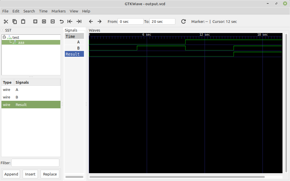
It is exactly what I expected to see: During the full simulation duration of 20ns Result goes to 1 only when A and B are 1, the very definition of an AND function.
Real hardware test
Now that simulation proved my design works I want to test it on real hardware.
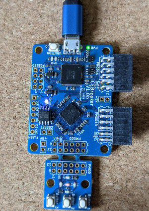
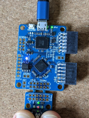
I have an open source development board named IceBreaker.
 Just by looking at the schematic I can identify a target for my module. I can use two buttons as inputs and one LED as output.
According to the diagram on the breakable part on the right side there are 3 buttons and 5 LEDs. On the main board there are 2 user-controllable LEDs and 1 usable button. I will create a text file with the FPGA pin mapping:
set_io LED_USR_RED 11
set_io LED_USR_GRN 37
set_io LED_RED     26
set_io LED_GREEN2  27
set_io LED_GREEN3  25
set_io LED_GREEN4  23
set_io LED_GREEN5  21

set_io BTN_USR     10
set_io BTN_1       20
set_io BTN_2       19
set_io BTN_3       18
I will save these mappings into a file named icebreaker.pcf because this happens to be the exact format expected by a place and route tool later on in the workflow.
I will use Button 1 and 3 (pins 18 and 20) and LED green 2 (pin 27). This is the modified module saved as test.v:
module top (
        input BTN_1,
        input BTN_3,
        output LED_GREEN2 );

        assign LED_GREEN2 = BTN_1 & BTN_3;
endmodule
Step 1: Synthesis
First step is to synthesize logic elements using the verilog model. The tool for this is yosys, official documentation can be found here: http://www.clifford.at/yosys/documentation.html. It can be used as an interactive tool by using its command prompt to issue commands but can also be used as an automatic generator.
Interactive mode
Test the interactive mode by starting yosys and issuing the following commands:
read_verilog test.v
hierarchy -top top
proc
opt
show
This is the abstract representation of my design, an AND gate:

FPGAs don’t really have logic gates but they simulate them by using lookup-tables. Easiest way to test this is to actually synthesize for a physical device and look again at the generated logic. Here are two commands which do this for the icebreaker chip:
synth_ice40
opt
show
 .
.
It synthesized a 4-input lookuptable with 2 hardcoded values and 2 variables (my buttons).
To verify functionality even more I quickly added a third button as input and modified the logic to take that into account making a three-input AND gate. This was the result:
To generate a diagram in SVG format you can use this command:
show -format svg -prefix test

The final stage is writing the result (netlist) in json format and exiting:
write_json test.json
exit
Non-interactive mode
Command to do this step will execute synth_ice40 step for the chip that’s on the Icebreaker board and will generate a json file with the result of synthesis.
yosys -ql yosys-output.log -p 'synth_ice40 -top top -json test.json' test.v
Results of the synthesis will be available in a file named “yosys-output.log” in the current folder.
Step 2: Place and route
For the chip I am using there are two options:
- Arachne PNR - No longer maintained, supports routing only for the chip family I am using
- NextPNR - The option going forward, better design and FPGA support.
The command to generate an ASCII representation of the result of P&R process is:
nextpnr-ice40 --pcf-allow-unconstrained --up5k --package sg48 --json test.json --pcf icebreaker.pcf --asc test.asc
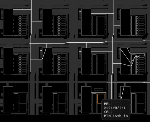
This will route the design, allocate lookup tables and connect them to the outside pins of the chip according to the icebreaker.pcf pin mapping I created earlier. The tool also has a QT-based gui really fun to play with which is accessible by adding “–gui” parameter at the end of the command above:
nextpnr-ice40 --pcf-allow-unconstrained --up5k --package sg48 --json test.json --pcf icebreaker.pcf --asc test.asc --gui
It will display a physical representation of the logic elements along with their configuration and interconnections. You can manually go through all the steps like pack, assign budget, place, route.
This is how it looks like for my simple AND example:
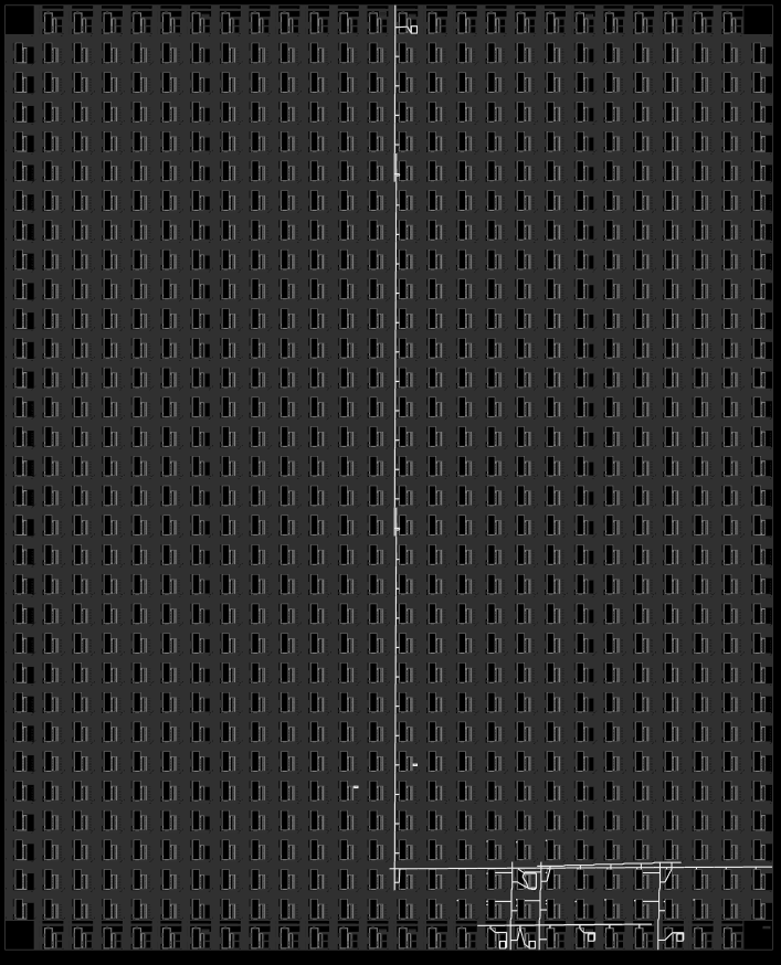
It can zoom in/out, display details about the lookup tables, pretty cool!
Step 3: Pack
FPGAs won’t understand this ASCII format of describing what cells are supposed to be configured as. No worries though, here comes icepack tool to the rescue. It reads the .asc file and convert it to a binary format specific to the chip I am using on the icebreaker board: ICE40 UltraPlus 5K. Usage couldn’t be simpler:
icepack test.asc test.bin
Step 4: Programming
Last step is to program the binary bitstream into the flash chip so the FPGA can read it and reconfigure itself every time power is applied. For this there is another tool named iceprog:
iceprog test.bin
Here is the result:
SUCCESS!
Using ninja build system
I like to use ninja build system instead of plain-old make. I happen to dig it’s simplicity and clarity so I created a build.ninja file to execute all these steps I talked about in this article.
rule synthesize
  command = yosys -ql yosys-output.log -p 'synth_ice40 -top top -json $out' $in

rule placeroute
  command = nextpnr-ice40 --pcf-allow-unconstrained --up5k --package sg48 --json $in --pcf icebreaker.pcf --asc $out

rule pack
  command = icepack $in $out

rule program
  command = iceprog $in

#--------------------------------------------------

build test.json: synthesize test.v

build test.asc: placeroute test.json

build test.bin: pack test.asc

build prog: program test.bin
Building could not be simpler, just issue “ninja” command in the project folder.
Cleaning up can also be done using “ninja -t clean”
It is also able to generate graphs of its workflow using a command like this one:
ninja -t graph | dot -Tsvg -otest_ninja_graph.svg

Github link
All the sources are available on Github at the address:
https://github.com/z80-ro/verilog-tests/tree/master/00_test_the_tools